With the rapid development of integrated circuit manufacturing technology, small defects on the surface of the wafer during the manufacturing process will become the major obstacle affecting yield. Alfa Chemistry has in-depth research on the surface damage introduced in the back-end processing of wafers (such as slicing, grinding, lapping, polishing and chemical mechanical polishing). Alfa Chemistry is capable of providing wafer surface damage inspection services. Our inspection reports can effectively help customers conduct further research.
Alfa Chemistry Measurement Methods
To study residual damage, we commonly use optical microscopy, atomic force microscopy (AFM), scanning electron microscopy (SEM), transmission electron microscopy (TEM), X-ray characterization technique, and polarized laser scattering (PLS).
- Compared with typical XRD methods, X-ray characterization technology has higher sensitivity to measure surface damage. Due to its lossless nature and fast measurement time, this technology is particularly useful for optimizing every step in the back-end processing.
- The PLS method provides a more comprehensive inspection tool for SSD measurement during processing. The schematic configuration of the PLS system is shown in Figure 1.
 Fig 1. The schematic configuration of the polarized laser scattering system. (Yin J. F, et al. 2020)
Alfa Chemistry's Instrument Platforms
Alfa Chemistry has high-precision and repeatable advanced testing equipment, which can provide accurate and professional test reports. Our testing Instruments include, but are not limited to, the following:
- Scientifica SliceScope
- Malvern Panalytical X-ray Diffractometer
- LVEM5 Benchtop Electron Microscope
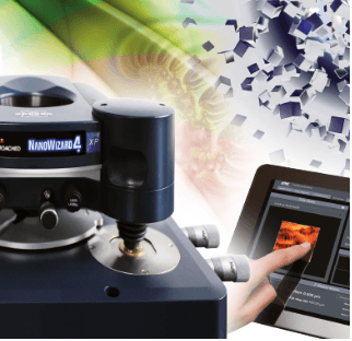
- NanoWizard 4 XP NanoScience AFM
Detectable Samples Include:- Wafer diameter: 150mm, 200mm, 300mm.
- Material: Si, GaAs, Ge, SiC, InP.
- Surface: Cutting, grinding, etching, polishing and patterned.
Testing Standard- SEMI-MF950 Test Method for Measuring the Depth of Crystal Damage of a Mechanically Worked Silicon Wafer Surface by Angle Polished and Defect Etching
- ASTM F950-1998 Test Method for Measuring The Depth of Crystal Damage on The Surface of Machined Silicon Wafers by Corner Polishing and Defect Erosion Processing Methods
- ASTM F1810-1997 Standard Test Method for Statistical Analysis of Silicon Wafer Erosion or Surface Defects
- KS D 0261-2012 Appearance Inspection of Mirror Silicon Wafer
References
- Yin J. F, et al. (2020). "Two-Dimensional Detection of Subsurface Damage in Silicon Wafers with Polarized Laser Scattering." Journal of Materials Processing Tech.284: 116746.
- Letts E, et al. (2018). "X-Ray Characterization Technique for The Assessment of Surface Damage in GaN Wafers." Journal of Crystal Growth. 501: 13-17.


