What is a Sputtering Target?
A sputtering target is a material generated by PVD to form thin films. In sputtering, an ion beam hitting the surface of the target dislodges atoms or molecules from the target and spews them off into a substrate in a thin film. A sputtering target normally consists of a target blank and backing plate. The target blank is the sputtering target's central part and is the material that the super-fast beam of ions directly hits.
Industrial Chain of Sputtering Targets
Four stages comprise the sputtering target manufacturing chain, metal purification, target manufacture, sputter coating and end-use applications.

Characteristics of Sputtering Targets
High Purity and High Density: Sputtering targets usually need to be high purity and high density to sputter excellent quality thin films. For instance, purity can be anywhere between 2N and 6N for sputtering targets, materials might be Ni, Co, Fe, Cr, Mo, Ta, Ag, Gd, Tb, Al, Ti, V, Zr, Hf, etc.
Multi-component and Grain Uniformity: Sputtering targets usually consist of a target blank and backing plate, the target blank being the core. The smaller the grain size of the object, the faster the sputtering speed; the larger the grain size, the more even the distribution of film thickness following sputtering.
Variety of Materials and Shapes: There are different metal targets (like copper, aluminum, molybdenum), alloy targets (like copper-manganese alloys) and ceramic targets (like zinc oxide aluminum). There are targets with shapes: planar targets (Long, square, and circular) and rotating targets (Tube), with various uses, features, and drawbacks.
Good Electrical and Thermal Conductivity: Metal targets (like copper) are used extensively in integrated circuits and microelectronic equipment as they have good electrical and thermal conductivity. Ceramic targets are for applications at extreme temperatures and in corrosive environments, as they have very good chemical stability and high melting points.
Categories of Sputtering Targets
Metal Targets: These are all pure metals like aluminium (Al), copper (Cu), titanium (Ti), molybdenum (Mo), etc. These targets are usually applied in the preparation of conductive and barrier layers for semiconductor devices.
Alloy Targets: Constructed using 2 or more metal components such as copper indium gallium selenide (CIGS) targets, Nickel-chromium alloy targets,Titanium-Aluminum targets,etc. These targets are better in terms of mechanical stiffness, resistance to corrosion or specialised electromagnetic properties.
Ceramic Compound Targets: Including oxides, silicides, carbides, etc., such as ITO targets, common on flat-panel displays and thin-film transistors (TFT) for flat-panel displays.
Preparation Technology of Sputtering Targets
Sputtering targets are a time-consuming, elaborate, highly accurate manufacturing process consisting of material selection, melting, moulding, cutting, cleaning, and packaging in general; to manufacture pure metal targets, these processes generally go like this:
1. High purity metal raw materials are selected and melted into liquid form at high temperatures by vacuum melting or electron beam melting to keep the target high purity and homogeneous.
2. The substance is poured into blocky objects by means of molds or casting.
3. The targets are then precisely cut to the target size and shape and the surface pollutants are removed during a careful cleaning operation.
4. Finally, the targets are packaged to prevent oxidation and contamination.
Impact of High-Purity Targets on Film Properties
Reducing Impurity Levels in Thin Films: Purity targets are important for thin films to work well. They can make the films with significantly less impurity. Film contaminants could create defects, reduce crystallinity or change phase compositions, which could deteriorate the film conductivity, optical properties, mechanical properties, etc. If the target of high purity and preparation are regulated, then the impurity can be reduced which will give the thin films more purity and better performance.
Ensuring Consistency of Film Composition: High-purity targets also maintain consistency of the thin films structure. When a film is deposited, its composition and microstructure on the target surface may alter with time due to sputtering, which can affect the film composition and characteristics. Choosing targets of high purity and regularly reusing them to keep the surface state fresh can guarantee reproducibility of the film composition.
How to Maintain High Purity, Uniformity, and Density of Targets?
The goal of achieving purity, uniformity, and density in targets would require to eliminate impurities from raw material, and not introduce new impurities in preparation process. Uniformity is the same as consistency in the performance of the target at various components — it involves blending raw materials in the same proportion and control over the temperature when melting. Density determines the efficiency of sputtering and the film quality, which can be optimized by shaping it and treating it accordingly.
In pursuit of these aims, scientists are continuously developing new purification technologies and process optimization strategies. In some high-tech methods, such as vacuum melting, electron beam refining, and zone refining, impurities are able to be removed from the target. A thorough raw material selection, production process control, and final product testing all help to make sure the purity of the target is equivalent or better than industry standards.
How to Select the Right Target Material
The target material selection involves a detailed review of applications, material properties, chemical purity, cost-effectiveness, processability and availability of supply. Below is a detailed analysis:
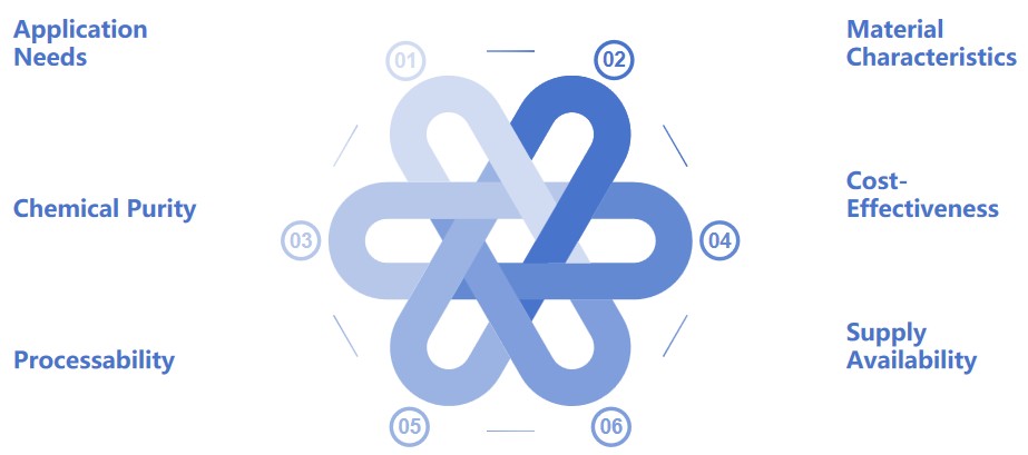
Application Needs: First of all, one must know the target material will be applied to (physical vapor deposition (PVD) or magnetron sputtering, as this dictates what materials are needed for. In the case of semiconductors, for instance, the target material selected directly influences the properties of the thin films.
Material Characteristics: The material specificity and type of the material chosen matters a lot. The most typical target elements are metals, oxides and alloys, which each have different physical and chemical characteristics for different purposes. Metal targets like copper and aluminum, for example, are very conductive and can be used in semiconductor and electronics applications, whereas ceramic targets like aluminum oxide are better suited to extreme temperature and corrosive conditions.
Chemical Purity: High-purity standards are key to obtaining quality thin films especially for applications in microelectronics and optics where impurities adversely affect conductivity and optical transparency. Hence the use of high purity materials is necessary to keep impurity release to a minimum and further increase the film quality and performance.
Cost-Effectiveness: Cost and performance are the primary considerations while making sure the material is up to specs. Good materials may be more expensive, so there's no one answer that's both suited to the job and economically viable.
Processability: Processability of the material to be considered as well, as well as it compatibility with the required dimensions, shape and equipment. For instance, the density and uniformity of the target determines the stability of the deposition process, while high density can reduce the likelihood of holes in the film and hence the effectiveness of deposition.
Supply Availability: Stable supply of the target material chosen is vital so you must select long-term reputable suppliers to assure the supply and quality throughout.
In conclusion, selecting the right target material requires considering application needs, material characteristics, chemical purity, cost-effectiveness, processability, and supply availability to ensure optimal performance and long-term stability.
Applications of Sputtering Targets
Sputtering targets are useful in many areas, such as:
Semiconductor Manufacturing: Sputtering targets are necessary materials for the manufacture of semiconductor chips. Targets are applied to metal wiring, dielectric and protective coatings to be added to wafers and chip packages. Copper, aluminum, molybdenum and ITO targets, for instance, are some of the most popular semiconductor targets.
Flat Panel Displays: Sputtering targets are also employed in flat panel display (e.g., LCD, OLED). These targets are used to create the thin films needed for liquid crystals and touch screens. For instance, transparent conductive films are produced with ITO targets.
Solar Cells: In a solar cell manufacturing process, the sputtering targets deposit light-absorbing films and other functional films to increase the efficiency of the cell's photoelectric conversion. Targets made from zinc aluminum oxide (AZO), for instance, are widely used in the production of solar cells.

Optical Applications: Sputtering targets are also employed in optical products such as optical filters, precision optical equipment and laser lenses which demand transparent thin films with certain optical properties.
Energy Sector: Sputtering targets are used to manufacture solar panels and gas turbine blade coatings to enhance component's efficiency and durability.
Decoration and Industrial Applications: Sputtering targets are also used to apply surface finishes to phone, watches, glasses, etc for improved appearance and durability. They are also used to strengthen surface of molds and glass finishes.
Medical and Scientific Research: Sputtering targets are applied to medical instruments and implants to form thin films, making them biocompatible and functional. In research, sputtering targets are used to make microanalysis samples slides and microscope parts.
Laser Technology: Sputtering targets enable thin films for fiber lasers and semiconductor lasers, the fundamental elements of laser devices.
In short, the range of applications for sputtering targets is vast, and ranges from high-tech electronics to household products. They depend not just on the material, but also on the support of the new sputtering technologies and machinery.
Reference
- Liang, G., et al. "Spark plasma sintering of Sb2Se3 sputtering target towards highly efficient thin film solar cells." Solar Energy Materials and Solar Cells 211 (2020): 110530.

